Masonlar.org - Harici Forumu


Gönderen Konu: Intel Transistors Enter the Third Dimension  (Okunma sayısı 3355 defa)

0 Üye ve 1 Ziyaretçi konuyu incelemekte.

Mayıs 09, 2011, 07:47:57 ös
  • Aktif Uye
  • ***
  • İleti: 574
  • Cinsiyet: Bay


RACHEL COURTLAND

From what I remember of Honey, I Shrunk the Kids, getting zapped by Wayne Szalinski’s shrink ray was not a cause for celebration. But Intel senior fellow Mark Bohr, who submits to a virtual miniaturization process that leaves him 100nm tall, seems positively gleeful in this new video from the company.

Bohr is celebrating Intel’s new, smaller, and, for the first time, three-dimensional transistor. Dubbed Tri-Gate, the device employs a much-anticipated design innovation – multiple gates that wrap around a raised silicon channel.
The transistors will appear in Intel's new "Ivy Bridge" microprocessor, which will be made using a 22nm manufacturing process and begin shipping later this year. Intel's processor is the first make the jump from 32nm to 22nm, continuing the decades-long race to keep boosting the number of transistors that can be packed into the same amount of space.

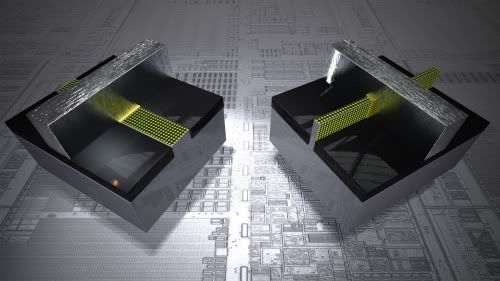
The switch to 3D addresses some fundamental problems that have been plaguing transistors as their feature size has shrunk. Transistors have long been two-dimensional affairs, with a source and a drain separated by a channel along which electrons flow. The only components that sit above the plane are the gate, which turns on and off the flow of electrons, and a thin, insulating layer sandwiched between the gate and the channel.

But as engineers have made transistors smaller and smaller, the distance from the source to the drain has gotten so short that electrons can leak through the lower part of the channel, where the gate's influence is weakest, wasting power. To solve the leakage problem, transistor designers have been eyeing three-dimensional designs in which electrons have no place to go that isn’t controlled by the gate.
Intel’s solution is a FinFET design that employs a ridge-like silicon channel that juts out of the silicon substrate. The transistor’s gate runs perpendicular to the channel and drapes over it, creating three gates around the channel.

Intel reports its new 3D, 22nm transistors are 37 percent faster at low voltage compared to Intel's current 32nm planar transistors, making them better for smartphones and other handheld devices. They draw less than half the power as the firm’s 32nm chips.

Despite that, the New York Times says, some think Intel is making a gamble, because alternative approaches may offer better gains on the power front:
There has been industry speculation that FinFET technology will give Intel a clear speed advantage, but possibly less control over power consumption than alternative approaches...The scope of Intel’s gamble is underscored by the fact that while the company dominates in the markets for data center computers, desktops and laptops, it has largely been locked out of the tablet and smartphone markets which are growing far more quickly than the traditional PC industry.
Intel made a tentative step into the low power market last month, with the introduction of its first processor for tablet computers.


« Son Düzenleme: Mayıs 09, 2011, 08:31:54 ös Gönderen: poyraz06 »


Mayıs 09, 2011, 07:57:10 ös
Yanıtla #1
  • Aktif Uye
  • ***
  • İleti: 574
  • Cinsiyet: Bay


Intel, önümüzdeki sene kullanıma sunacağı Ivy Brige mimarisinde kullanılacak devrim niteliğindeki yeni transistör teknolojisini tanıttı. Artık işlemcilerde 3D transistörler bulunacak.

İşlemci teknolojisinde öncü olmasıyla bilinen Intel, önümüzdeki yıl piyasaya süreceği Ivy Bridge kod adlı işlemci mimarisinde kullanılan yeni bir teknolojiyi tanıttı.

22 nm’lik transistörlere sahip olacak Ivy Bridge modellerinde Intel, transistör yapısını değiştirerek hem performans, hem de güç tasarrufu konusunda önemi bir aşama kaydetmiş.

3D transistör olarak adlandırılan yeni transistörlerde öncekilerden farklı olarak Tri-Gate adı verilen bir yapı bulunuyor.

Elektronlar Tri-Gate’ten Geçecek

Transistör üzerinden geçen elektrik akımını iki boyutlu bir yüzey yerine üç boyutlu bir yapı içinden geçirmeyi başaran Intel mühendisleri, 22 nm’lik bu yeni transistörlerde çok daha iyi performans elde edebilmişler.

Intel geliştirdiği yeni teknolojiyi ilginç bir animasyonla tanıttı. Videoda, şirketin üst düzey yetkililerinden Mark Bohr transistörlerle aynı boyuta getirilerek yeni teknolojiyi yakından görmemizi sağlıyor.

Video Animation: Mark Bohr Gets Small: 22nm Explained


(ShiftDelete.net)
« Son Düzenleme: Mayıs 09, 2011, 08:31:16 ös Gönderen: poyraz06 »


Mayıs 09, 2011, 08:39:12 ös
Yanıtla #2
  • Seyirci
  • Aktif Uye
  • ***
  • İleti: 647
  • Cinsiyet: Bay

22 nanometreye inebilmeleri büyük başarı, zaten 40 nm ile AMD'nin önünde yer alıyorlardı. Ancak daha fazla elektron daha fazla direnç demektir. Daha fazla direnç, ısı ve enerji kaybı demektir. Üstelik elektronların 2 boyutta yol aldığını ilk defa duyuyorum. Tabi tam yapısını göremediğim için bir şey söylemek çok güç. Bu konu açıkçası şimdilik pek inandırıcı gelmedi. Bekleyip görmek lazım.

Saygılarımla...
Bir yere ait olmayı hiç istemedim. Ya kendim olurum yada başkalarının arkamdan övgüleri ile ölmüş olurum.


Mayıs 10, 2011, 12:18:37 öö
Yanıtla #3
  • Aktif Uye
  • ***
  • İleti: 574
  • Cinsiyet: Bay

Tamamen bitirdiklerinde daha ayrıntılı bir açıklama gelir ben de burada paylaşırım :) Bunun dışında, Intel'in asıl hedefi 11nm ye inmek. Bakalım neler olacak :)


Mayıs 26, 2011, 05:53:56 ös
Yanıtla #4
  • Seyirci
  • Aktif Uye
  • ***
  • İleti: 647
  • Cinsiyet: Bay

Siz biliyor musunuz bilmiyorum ama, transistörler ufaldıkça bir sorun çıkıyor, yalıtım. O kadar küçük bir alanda  o kadar küçük akımlar söz konusu oluyor ki, yalıtım malzemesi bile sorun yaratıyor. Sanırım böyle bir yalıtım için 3m kalınlığında bir duvar gerekiyormuş. :)
Bir yere ait olmayı hiç istemedim. Ya kendim olurum yada başkalarının arkamdan övgüleri ile ölmüş olurum.


Haziran 08, 2011, 10:59:14 ös
Yanıtla #5
  • Ziyaretçi

Aslında 3 boyutlu işlemciler tasarım ve prototip olarak 3-5 senedir var. Ancak seri üretim olarak o boyutlarda 3 boyutlu işlem kapasitesini oluşturmak sorundu. Intel bunu başarmışsa helal olsun derim!...

Ancak şu var ki gerçek anlamda 3 boyutlu işlemci bir küre gibidir, veri iletiminde, transistorler arası elektrik iletimi/elektron akışı gibi performans faktörlerinde, düzlemsel işlemcilere göre bir anda onlarca hatta yüzlerce kat daha fazla hız ve performans sağlar (sağlaması beklenir). Zannederim ki Intel, bu yolda teknik olarak küçük bir ilerleme ile çok daha gelişmiş bir mimarinin önünü açıyor....

saygılar